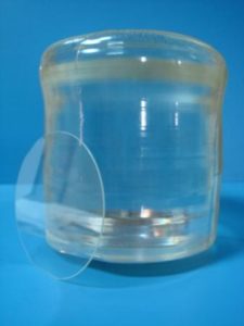
Introduction of LiNbO3
LiNbO3 is widely used as electro-optic modulators and Q-switches for Nd:YAG, Nd:YLF and Ti:Sapphire lasers as well as modulators for fiber optics. The following table lists the specifications of a typical LiNbO3 crystal used as Q-switch with transverse E-O modulation. The light propagates in z-axis and electric field applies to x-axis. The electro-optic coefficients of LiNbO3 are: r33 = 32 pm/V, r31 = 10 pm/V, r22 = 6.8 pm/V at low frequency and r33 = 31 pm/V, r31= 8.6 pm/V, r22 = 3.4 pm/V at high electric frequency. The half–wave voltage: Vπ=λd/(2no3r22L), r c=(ne/no)3r33-r13.
LiNbO3 Q-Switch Specifications
| Size | 9 X 9 X 25 mm3 or 4 X 4 X 15 mm3 |
| Other size is available upon request | |
| Tolerance of size | Z-axis: ± 0.2 mm |
| X-axis and Y-axis:±0.1 mm | |
| Chamfer | less than 0.5 mm at 45° |
| Accuracy of orientation | Z-axis: <± 5’ X-axis and Y-axis: < ± 10’ |
| Parallelism | < 20″ |
| Finish | 10/5 scratch/dig |
| Flatness | λ/8 at 633 nm |
| AR-coating | R < 0.2% @ 1064 nm |
| Electrodes | Gold/Chrome plated on X-faces |
| Wavefront distortion | <λ/4 @ 633 nm |
| Extinction ratio | > 400:1 @ 633 nm, φ6 mm beam |
LiNbO3 is also a good acousto-optic crystal and used for surface acoustic wave (SAW) wafer and A-O modulators. Photonchina provides acoustic (SAW) grade LiNbO3 crystals in wafers, as-cut boules, finished components and custom fabricated elements.
Typical SAW Properties
| Cut Type | SAW Velocity Vs (m/s) |
Electromechanical Coupling Factor k2s (%) |
Temperature Coefficient of Velocity TCV (10-6/oC) |
Temperature Coefficient of Delay TCD (10-6/oC) |
| 127.86o Y-X | 3970 | 5.5 | -60 | 78 |
| Y-X | 3485 | 4.3 | -85 | 95 |
Typical Specifications
| Type Specifications | Boule | Wafer | ||
| Diameter | Φ3″ | Φ4″ | Φ3″ | Φ4″ |
| Length or Thickness(mm) | ≤100 | ≤50 | 0.35-0.5 | |
| Orientation | 127.86°Y, 64°Y, 135°Y, X, Y, Z, and other cut | |||
| Ref. Flat Orientation | X, Y | |||
| Ref. Flat Length | 22±2mm | 32±2mm | 22±2mm | 32±2mm |
| Front Side Polishing | Mirror polished 5-15 Å | |||
| Back Side Lapping | 0.3-1.0 mm | |||
| Flatness (mm) | ≤ 15 | |||
| Bow (mm) | ≤ 25 | |||
Size and specification of wafers upon request is available.
