Introduction of Silicon Wafer
Silicon is the second most common element on earth and the seventh-most common element in the entire universe. It is the most common semiconductor and the most widely used in the electronic and technology sector.
Application of silicon wafers span different types of industries: computing, solar cells, semiconductors and optics.
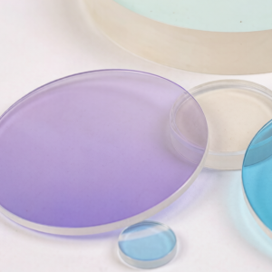
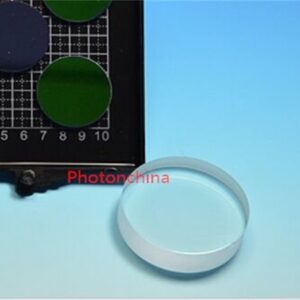
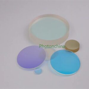
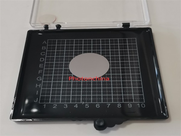
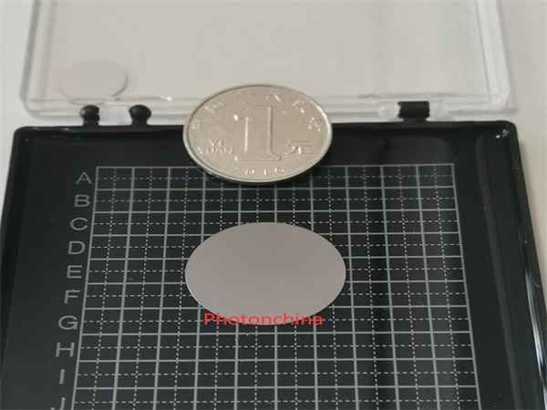
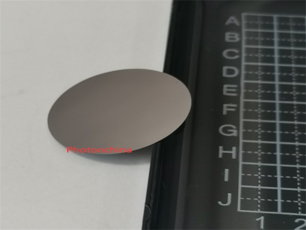
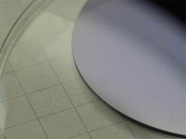
In the field of optics, silicon is an economic IR material. Polished Silicon wafers are specifically manufactured to meet optical grading. They find usage in both fiber optics and micro-optic devices worldwide.
In the field of fiber optics and precision micro-optic devices, we are the leading manufacturer of the thinnest silicon wafer/window in the world, reaching 0.05mm(50 micro) in thickness, with the high tolerance of +/-0.002mm, for 25.4mm(1 inch) diamter.
Silicon can be produced as either mono or polycrystalline form by Czochralski crystal growth method or float zone method. CZ Silicon is cheaper. But it contains some oxygen that induces an absorption band at 9 microns. Optical grade silicon is generally lightly doped, and has a very good transmission from 1.2um to 7um. Dopant is usually boron (p-type) or phosphorus (n-type), and both types are acceptable for IR applications.
Apart from optical grade silicon wafer, Photonchina also offers silicon wafer to SEMI standards for other applications as well.
Specifications:
| Crystal Growth Method | Czochralski (CZ) or Float Zone (FZ) Method |
| Orientation | <111>, <100> or Random Orientation |
| Diameter | 1 inch, 2 Inches, 3 Inches, 5 Inches, 6 Inches etc. |
| P type Dopant | Typical Boron |
| P type Resistivity | Typical 5 ~ 100 ohm/cm |
| N type Dopant | Typical Phosphorus |
| N type Resistivity | Typical > 10 ohm/cm |
| Thickness | 500±30µm, 1000±50µm |
| Surface Quality | 40-20, 60-40, 80-50 |