Introduction of CaF2
Calcium fluoride (CaF2), a colorless cubic crystal, is insoluble in water. It is one of the few natural crystals that exist in nature. Because of its good optical properties, calcium fluoride crystal has the advantages of wide light transmission range, high transmissivity, low refractive index, and large relative dispersion, showing important applications in the optical industry.
Calcium fluoride crystal has the characteristics of high transmittance and very high laser damage threshold in deep ultraviolet region. It is widely used as windows, lens, prism, beam splitter, substrate material, etc. from vacuum ultraviolet to mid infrared band. High purity calcium fluoride single crystal is a good window material for excimer lasers in vacuum ultraviolet band, and single crystal or hot forged single crystal is a suitable window material for chemical like carbon monoxide lasers.
The good optical properties of calcium fluoride crystals in vacuum band are incomparable with other materials. The calcium fluoride crystals used in this band also have the advantages of radiation resistance, high ozone resistance, corrosion resistance to fluoride gas, and low cost.
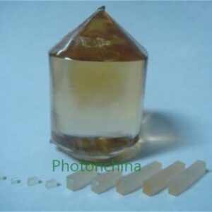
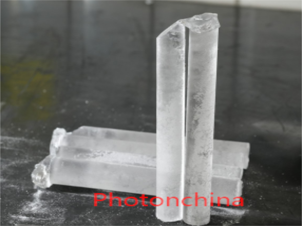
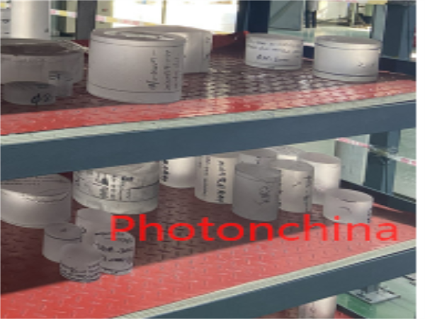
The growth of fluoride crystals mainly adopts the crucible lowering method and the pulling method. After that, Photonchina CaF2 blanks will go through the processes of rough grinding, fine grinding, cleaning, optical polishing, coating, inspection, etc., and finally they will be delivered to customers for use.
Basic definition of CaF2 materials
Monocrystal (single crystal): The particles inside the crystal are regularly and periodically arranged in the three-dimensional space, or the whole crystal is composed of the same spatial lattice in the three-dimensional direction, and the particles in the whole crystal are arranged in a long-term order in space.
Polycrystal (polycrystal): a collection of single crystals with many oriented grains. Both polycrystals and single crystals are based on the periodic structure of lattice. For the same variety of crystals, they are essentially the same.
Grain boundary: grain boundary is the interface between grains with the same structure but different orientations. On the crystal interface, the arrangement of atoms transits from one orientation to another, so the arrangement of atoms at the grain boundary is in a transitional state. The contact interface between grains is called grain boundary. In the appearance, it can be observed under light. The reflected light of the grain surface on both sides of the grain boundary is different, and the boundary is the grain boundary
Twin crystal: refers to the mirror symmetrical orientation relationship formed by two crystals (or two parts of a crystal) along a common crystal plane (i.e. a specific orientation relationship). These two crystals are called “twins”, and this common crystal plane is called twin plane.
Dislocation:
It can also be called differential arrangement. In materials science, it refers to an internal micro defect of crystal materials, that is, the local irregular arrangement of atoms (crystallographic defects).
Substructure: a kind of mosaic structure, generally referring to the dislocation arrangement and distribution inside the crystal; Specifically, the crystal is divided into subgrains with small orientation difference (from second to degree manitude), and the grain boundary can be attributed to the ranks or networks of dislocation (see dislocation). They are all relative to superstructures or modulation structures, and their cells are now called subcells.
Inclusions: The substance within the crystal that are different from the crystal materials. The package includes impurities and bubbles in the crystal, which can be observed by naked eyes under light.
Internal transmittance: refers to the transmission of crystal light by removing intrinsic absorption, front and rear surface reflection at a certain wavelength.
Optical homogeneity: indicates the degree of inhomogeneity of refractive index change of each part of the same crystal.
Stress birefringence: the birefringence phenomenon introduced due to the existence of residual stress in optical materials is called stress birefringence, and the stress birefringence is measured by the optical path difference in unit length. Stress birefringence is also called photoelastic effect.
Fluorescence: means a cold luminescence phenomenon of photoluminescence. When a substance at room temperature is irradiated by an incident light of a certain wavelength (usually ultraviolet or X-ray), it enters the excited state after absorbing the light energy, and immediately de excitation and emits an outgoing light longer than the wavelength of the incident light (usually the wavelength in the visible light band).
Bubbles and stripes:
All crystal and glass materials will have small bubbles or stripes; This is stipulated in the national standard. Photonchina only provides qualified and even excellent products that can meet requirements.
It should be noted that some bubbles and stripes can not be detected at the initial stage of production, nor can they be seen at the slice stage. Only after precision polishing can they be seen by experienced inspectors or precision testing instruments.
Scattering particles:
There are visible white spots and dots in the crystal material, which will emit light after being illuminated with a laser pen. These are absolutely unqualified products.
Inconsistent color or brightness:
The color problem is mostly due to the inconsistent acid-base ratio of the material during the cleaning process; the inconsistent brightness may largely be caused by the different crystal orientation or crystal structure. For example, the 111 direction may not be as bright or transparent as the 100 direction.
Material grade
1.VIR Grade.
- Application wavelength: 400nm – 7600nm
- Single crystal, polycrystalline, substructure: all available
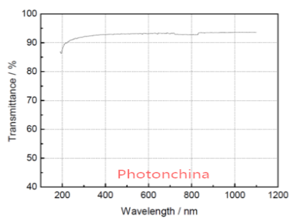
- Internal transmittance:>99.0% (10mm thick sample)
- Stress birefringence: PV 1 – 30nm/ cm@633nm
- Optical uniformity: PV 3- 50ppm@633nm
- Package: 25-125mW green light inspection, no visible light column, bubble, scattered particles, etc
2. UV Grade
- Application wavelength: 200nm – 400nm
- Single crystal, polycrystalline. Single crystal may have substructure
- Internal transmittance:>99.0% (10mm thick sample)
- Stress birefringence: PV 1 – 30nm/ cm@633nm
- Optical uniformity: PV 3- 20ppm@633nm
- There is no absorption peak at 205nm, and the absorption peak 306nm ± 5nm ≤2%
- Package: 25-125mW green light inspection, no visible light column, bubble, scattered particles, etc
3. VUV Grade
- Application wavelength: 130nm – 200nm
- Single crystal
- Transmittance:>50% @ 130nm,>80% @ 160nm,>85% @ 200nm (10mm thick product)
- Stress birefringence: PV 1nm/cm – 20nm/ cm@633nm
- Optical uniformity: PV 1- 15ppm@633nm
- Package: 25-125mW green light inspection, no visible light column, bubble, scattered particles, etc
4. IC Tool Grade, ICT Grade
- Application wavelength: 157nm, 193nm, 248nm, 355nm
- Single crystal
- Internal transmittance: 10mm thick sample, >99.8% @ 355nm, >99.8% @ 248nm, >99.7% @ 193nm, >99.4% @ 157nm, no absorption at 205nm and 306nm
- Stress birefringence: PV 2~10nm/ cm@633nm
- Optical uniformity: PV 3-20ppm@633nm
- Package: 25-125mW green light inspection, no visible light column, bubble, scattered particles, etc
5. Semiconductor laser grade (IC Laser Grade, ICL Grade)
- Typical indicators are consistent with the photolithography tool grade
- Laser tolerance: no standard to follow at present
- Laser damage threshold: ~7J/cm2 @ 193nm
6. Raman Grade
- Application wavelength: 130nm – 7600nm
- Single crystal polycrystal: single crystal
- Transmittance: 10mm thick sample, >50% @ 130nm,>80% @ 160nm,>85% @ 200nm, no absorption at 205nm and 306nm
- Stress birefringence: PV 2nm/cm~30nm/ cm@633nm
- Optical uniformity: PV 3-20ppm@633nm
- 25-125mW green light inspection: no visible light column, bubble, scattering particle, etc
- Fluorescence: no fluorescence in crystal
FAQs about CaF2 purchase
What are the available materials for UV band?
Monocrystalline or polycrystals are all available in Photonchina. Please feel free to let us know your applications by contacting our sales engineer.
Why is my UV CAF2 noisy?
The ultraviolet solar blind detector is required to be noiseless, but it requires coating at 200-400nm, typically R<0.5%
There could be many reasons for noise problem. It may be related to material itself, coating materials, or the bonding reaction between the material and the film.
We strongly recommend that you buy the finished products from Photonchina, as we provide from raw material, optical polishing, coating to final inspection.
Can polycrystal be used for D250mm and above?
From the perspective of growth, as long as the lattice is arranged within ± 5 degrees, it can be used as a single crystal. However, the thermal stress of the material is required to be low. At the same time, the temperature change must be controlled in the process of processing, and the size of the polish powder in the polishing process must also be strictly monitored, otherwise, there will be scratches, bad surface quality as well as flatness.
Can Photonchina provide Raman grade calcium fluoride?
Yes, we can supply Raman grade calcium fluoride. Please provide more detailed information on the application environment of materials.
Does calcium fluoride turn yellow after being used for a period of time?
It could happen. If the color of the lens surface turns yellow, it is typically due to the cleaning process while cutting and rounding. It can be wiped with alcohol or ether, or polished with polishing powder. If the color of the polished surface turns yellow after being used for a period of time, it is mostly caused by the internal absorption of the crystal, excessive laser energy or material fatigue caused by irradiation, which is an irreversible factor.
If there is a need in this regard, please raise this question in advance.
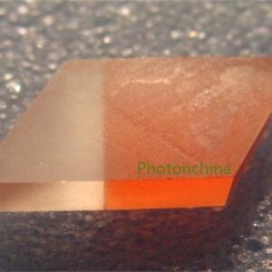
Why does calcium fluoride product look green?
Obviously, this is a material problem. Normal calcium fluoride is colorless and transparent crystal. Blue is a major defect in the material growth process, which is a nonconforming product.
It can be used in applications that do not have transmittance requirement.
Does single crystal product have a direction?
The single crystal must have a direction, but if not required, you could say all direction. All crystals with orientation are first single crystals, and then a specific diffraction angle is found for cutting. Therefore, the price of orientated single crystal is higher than one without orientation.
Why is 111 written on the calcium fluoride drawings?
The 111 direction is the main dissociation surface of calcium fluoride, which is also the best orientation among all directions. At the same time, it is noted in general literature. In theory, the optical performance of 111 is the best.
For ordinary system environment, there is no significant difference in performance, due to the isotropy of calcium fluoride. Therefore, most of the time, single crystal without orientation can be used in 111 direction.
Why is then 100/001?
It is marked for special use.
Does calcium fluoride with different crystal orientations affect polishing?
For ultra precision or ultra smooth products, it is recommended to use oriented products; Although others may have impact, they can be corrected through subsequent processing.
Why does the crystal have rather high stress?
Many reasons: the purity of raw materials is not good, the crystal process is not mature, the crystal equipment has problems, the crystal monitoring is not in place, the crystal cutting is too careless, and the whole production does not use the stress relieving process.
What does crystal stress affect?
The thermal stress too large, products will crack if the temperature changes sharply; Excessive mechanical stress, lens may encounter chamfering damage.
The greater the stress is, the poorer the uniformity of the material is. It will be difficult to make an excellent flatness and wavefront. At the same time, the refractive index of the lens could show slight difference.
Can stress be relieved?
Stress relief is only a relative concept; The thermal stress can be naturally released by placing for a long time, and will be gradually released in the subsequent cutting, grinding and polishing. The thermal stress crystal is most fully released during cutting. In fact, as long as it does not crack during cutting, the grinding and polishing will not crack. However, the mechanical and thermal stress generated by the rounding will not be eliminated in a short time. Therefore, most lenses have poor flatness at the edge and are required to have certain clear aperture area.
How to measure crystal stress?
Use stress instrument. Typically, the lens surface is polished and the aperture is set. The stress value is obtained by calculating the optical path difference.
What is the typical lead time for CaF2 products?
Basically, it would take 4 weeks to finish the whole production from grinding, polishing to optical coating.
The quantity, size and special requirement on products would have impact on time for production, however.
Recommendation for monocrystalline/polycrystalline application choice?
Single crystal products are recommended:
Complete sets of lenses, products with coating requirements, high-power laser products, and UV applications (such as high-power microscopes and cameras, having special demands such as wave plates, welding, birefringent crystals, etc.). High flatness products are required, PV<=1/ 10L@633NM.
Polycrystalline products are recommended:
Protection window, prism and other non-coated products; Gas analysis sensor, etc; Thermal imaging or products without requirements for imaging quality; Single lens for individual use.
Types of CaF2 available in Photonchina
1. Monocrystal (single crystal) CaF2 :
The particles inside the crystal are regularly and periodically arranged in the three-dimensional space, or the whole crystal is composed of the same spatial lattice in the three-dimensional direction, and the particles in the whole crystal are arranged in a long-term order in space.
Calcium fluoride (CaF2) crystals have high hardness, strong resistance to mechanical shock and thermal shock, and good transmissivity in the ultraviolet, visible and infrared fields. They are widely used in laser, infrared optics, ultraviolet optics, high-energy detectors and other scientific and technological fields. CaF2 crystal are especially known for their excellent optical performance in the ultraviolet band and is an ideal material for ultraviolet photodetectors, ultraviolet lasers and ultraviolet optical systems because of its high transmittance and low fluorescence radiation.
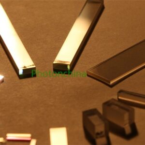
Shapes:
Lenses, Prisms, Wedges, Parts with hole, etc.
Basic parameters:
Diameter: 3mm-200mm, Thickness: 2mm-100mm
Diameter tolerance+0.1/-0.0mm; Thickness tolerance: ± 0.1mm
Grade: infrared, ultraviolet
Wavelength:130nm-10um
Scratch & Dig: 40-20, 60-40
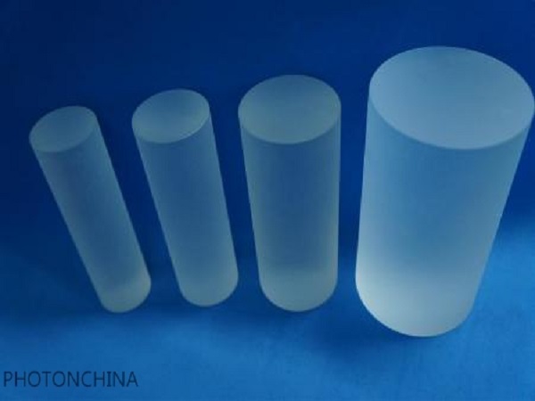
2. Polycrystalline (polycrystal) CaF2:
A collection of single crystals with many oriented grains. Both polycrystals and single crystals are based on the periodic structure of lattice. For the same variety of crystals, they are essentially the same.
The transmissivity of CaF2 polycrystals is the same as that of single crystals, and the chemical properties have no difference. The mechanical properties in physical aspects are not significantly different from that of single crystals, but the optical delay performance is not as good as that of single crystals.
Because of the homogeneity of calcium fluoride and the high output of polycrystals, we recommend it when you choose it to serve as protection windows, single lenses, or single prisms. However, for high-power lasers, single crystals are ideal solution.
Shapes:
Lenses, Prisms, Wedges, Parts with hole, etc.
Basic parameters:
Diameter: 3mm-450mm, Thickness: 2mm-100mm
Diameter tolerance+0.1/-0.0mm; Thickness tolerance: ± 0.1mm
Grade: infrared, ultraviolet, deep ultraviolet.
Wavelength:130nm-10um
Scratch & Dig: 40-20, 60-40
3. Ultraviolet CaF2
The ultraviolet calcium fluoride band is 200-400nm. The typical spectral characteristics are that there is no obvious absorption at 205nm and 306n, while the transmission in infrared band is not reduced. UV single crystal is mostly found in solar blind detector 260-280nm or UV imaging plays an achromatic role, making the noise lower and the image quality better. They are also used in ultraviolet vacuum observation window or spectral analysis. Ultraviolet CaF2 usually made of high purity chemical synthetic materials. It is required to control the absorption of cerium and lead in crystal growth and must conform to ROHS&REACH standards. Some natural ores can meet the requirements after strict screening, but they are not recommended, due to the fact that the consistency and stability of the materials cannot be guaranteed.
Shapes:
Lenses, Prisms, Wedges, Parts with hole, etc.
Basic parameters:
Diameter: 3mm-450mm, Thickness: 2mm-100mm
Diameter tolerance+0.1/-0.0mm; Thickness tolerance: ± 0.1mm
Grade: ultraviolet; Crystal structure: Single crystal, Poly crystalline.
Wavelength:200-400nm,200nm-1100nm
Scratch & Dig: 40-20, 60-40
4. Fluorescent-free Raman grade CaF2
Fluorescence-free CaF2 is a relative concept and is also called Raman grade calcium fluoride. The generation of fluorescence is due to the fact that the element composition of the crystal material itself contains a fluorescence source, or the defects generated in the material growth process. Fluorescence will cause strong absorption, resulting in energy loss, signal distortion or imaging disorder. Photonchina can grow and process non-fluorescent calcium fluoride crystals to meet the diverse needs of customers.
Basic parameters:
Diameter: 3mm-200mm, Thickness: 2mm-100mm
Diameter tolerance+0.1/-0.0mm; Thickness tolerance: ± 0.1mm
Grade: Ultraviolet,Infrared; Crystal structure: Single crystal.
Wavelength:200-400nm,200nm-1100nm
Scratch & Dig: 40-20, 60-40
5. Oriented CaF2
Calcium fluoride belongs to high grade cubic crystal system, which is typically isotropic. In practical applications, complex and high-precision photoelectric systems, high-power lasers, gyroscopes or high-precision microscope lenses, calcium fluoride with specific orientation has become the preferred solution considering the subtle differences in materials and the cumulative errors in material processing. Photonchina provides oriented CaF2 to customers worldwide.
Basic parameters:
Diameter: 3mm-200mm, Thickness: 2mm-100mm
Diameter tolerance+0.1/-0.0mm; Thickness tolerance: ± 0.1mm
Grade: Ultraviolet,Infrared; Crystal structure: Single crystal.
Wavelength:200-400nm,200nm-1100nm
Scratch & Dig: 40-20, 60-40
Crystalline Orientation: <111> <110> <100> <001> <220> etc.